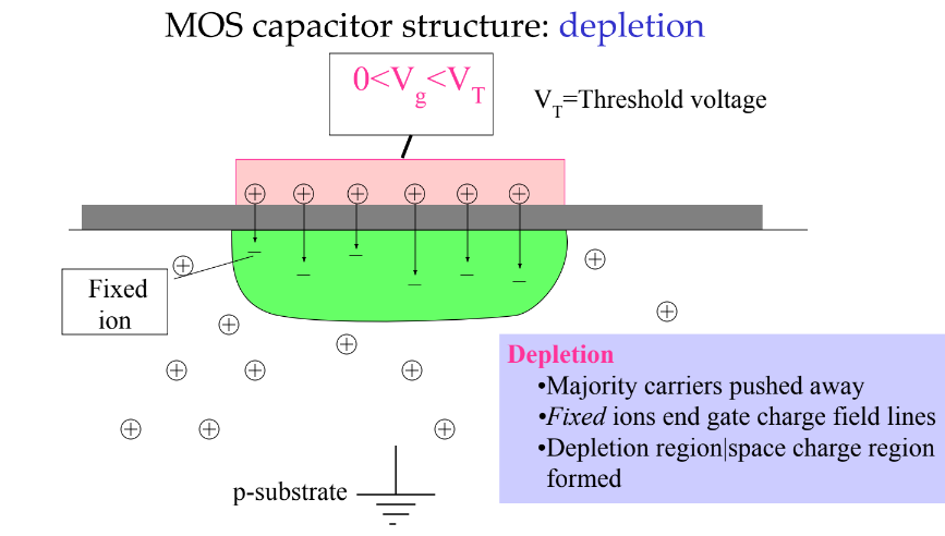
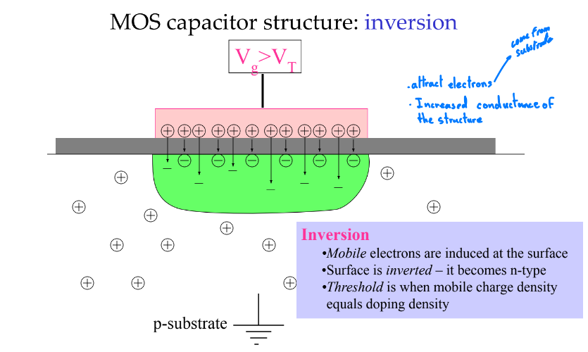
Structure
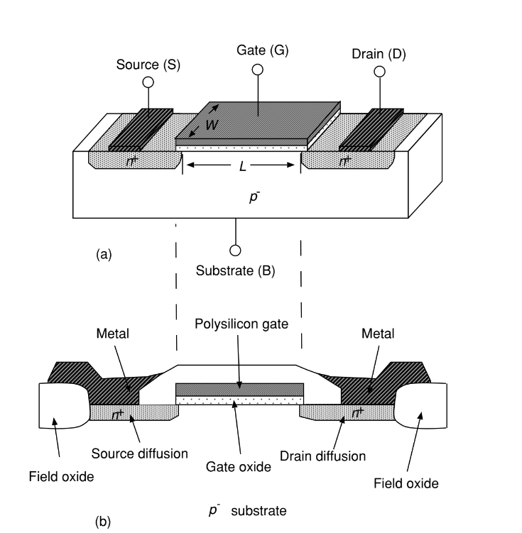
The MOSFET is composed of a MOS structure and two pn junctions. The source and drain are heavily doped n type (electrons are the majority carriers) and therefore have low resistivity. The channel is isolated from the gate by a layer of $SiO_{2}$. The gate is made of heavily doped polycrystalline silicon (low resistivity).
We can view the transistor as having four terminals; the gate (G), the source (S), the drain (D), and the bulk (B). Because the n+ source and drain regions can supply a lot of electrons to the channel, the device is called an n-fet. The complementary type is the p-fet (charge carried by holes from source to drain).
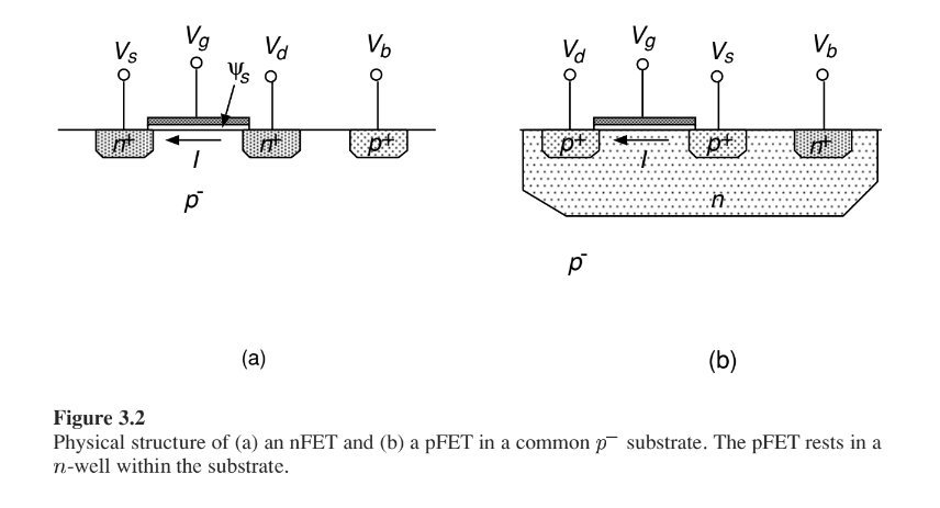
Almost all modern MOS processes are CMOS (Complementary Metal Oxide Semiconductor) In a CMOS process, both nFETs and pFETs are fabricated on the same substrate. Usually, we will assume a single well CMOS process in which the nFET rests in the common p- substrate, and the pFET rests in an n-well within the substrate.
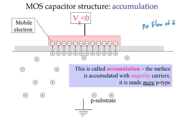
Accumulation
If the semiconductor is n-type, a positive charge on the conductor increases the majority carrier density near the semiconductor surface,an effect known as accumulation.
Flat band
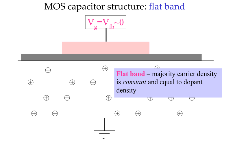
When there is no applied bias, the work functions of the semiconductor and the metal
are equal: the Fermi levels line up and the energy bands in the semiconductor are flat (flat-band condition).
Depletion
A negative charge on the conductor reduces the majority carrier density. With increasing negative charge on the conductor, most majority carriers are driven from the region near the surface, resulting in depletion, and eventually minority carriers start to accumulate at the semiconductor surface, an effect called inversion.