Semiconductors
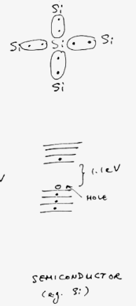
Crystals and other solids are classified by their electrical conductivity into insulators,Semiconductors,or metals (order of increasing conductivity). Electrical processing structures are fabricated from semiconductors because they operate at an intermediate conductivity level that can be modulated by impurity doping.
The classification of these materials also relies in the arrangement and propreties of the atoms.
Electrical currents in solids are carried by the motion of valence electrons, which are attracted from the fixed positive ion cores. An electron is either fixed to this core or mobile and contributes to the current flow (but only if it has enough energy to break free from the core (ionization energy)).
An intrinsic semiconductor is undoped
An extrinsic semiconductor is doped
Energy bands
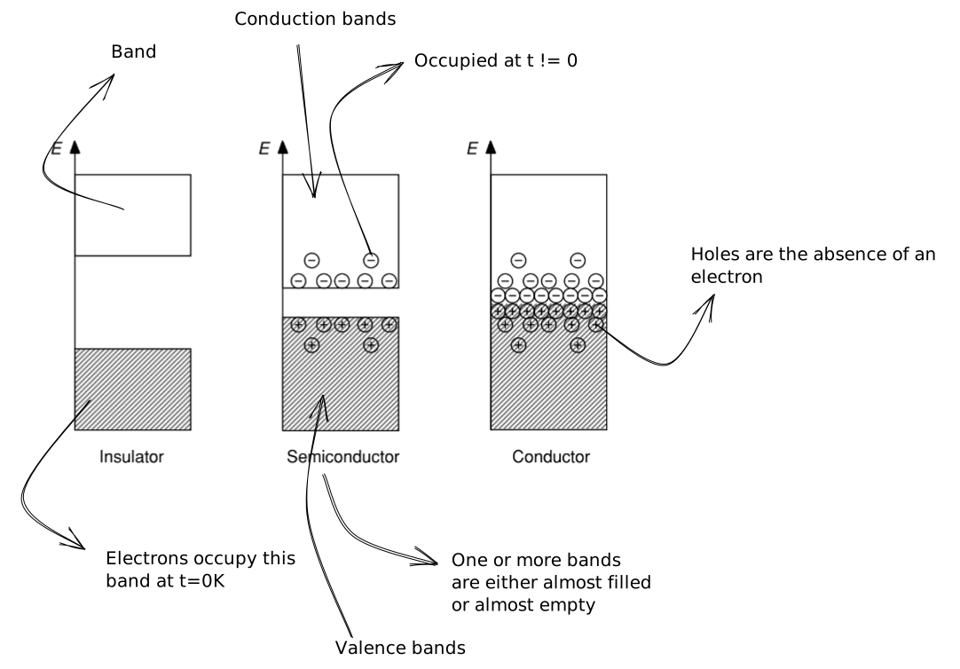
The electrons that are in solids can have different energy levels (free ones can be in any energy state), that are separated by forbidden zones band gaps (due to interaction with ion core). The allowed levels are called energy bands.
Each state can support a limited number of states each of which can be occupied by an electron or not at a given time.
%%🖋 Edit in Excalidraw, and the dark exported image%%
The energy bands are classified into valence bands and conduction bands according to whether they are almost filled or almost empty.
note: bands depend on the crystal structure
In conduction bands electrons are free to move, but in valence bands they are bound to the atom body and can only move from one unoccupied state to another if they cannot acquire enough energy to jump the bandgap to the conduction band.
Holes
Unoccupied states in valence bands are referred to as holes. Valence bands can be considered as conduction bands for holes. They are attributed a positive charge and mass and mobility.
Representation (Energy band diagrams)
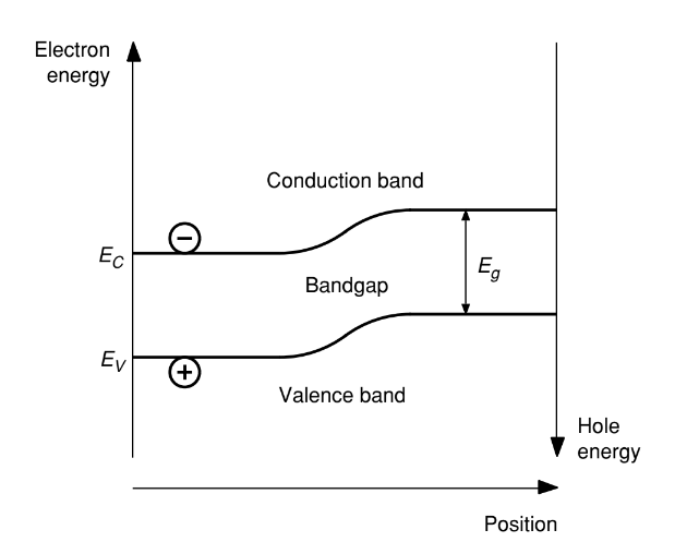
Energy band diagrams are drawn such as the electron energy increases upwards in $eV$ (electron volt). This unit is practical because by dividing by $-q = -1.60218 \times 10^{-19}C$ (electron charge) we can obtain an electrostatic distribution.
- Only the valence band and conduction band are drawn with the smallest energy separation.
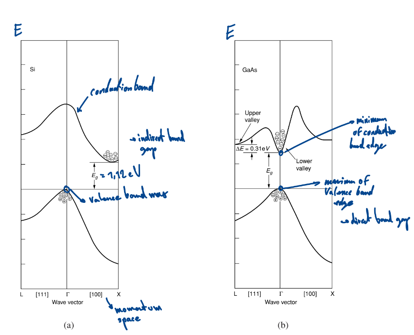
- The lines are the band edges, the highest valence band energy states and the lowest conduction band energy states. They tell us the minimum ampunt of energy an electron must acquire to bridge the gap (for a given change in momentum).
- $E_{g}$ is the bandgap energy (differenc between lowest conduction and highest valence band). For $Si, E_{g}=1.12eV$
- If the max-min occurs at the same wave vector, we speak of direct bandgamp ($GaAs$), if not we speak of indirect bandgamp ($Si$).
Simplified graph
Carrier concentrations
Thermal energy translates in vibrations of the crystal lattice. Transfer of energy from the lattice to the electrons is through absorption/emission of a phonon.
0 temp:
All low energy states are filled and high energy states are empty
High temp:
Some electrons leave the low E state for the high E states. The probability of occupation of these states is described by the Fermi-Dirac distribution. The probability that an energy state of value E is occupied is given by:
$F(E)=(1+e^{(E-E_{F})/kT})^{-1}$
Where,
- $E_{F}$ is the enrgy at which the occupation probability is $0.5$ (Fermi level)
- $k = 1.38 \times 10^{-23}J/K$ (Boltzmann constant)
For typical impurity doping concentrations and bandgaps of commonly used semiconductors $E_{F}$ is well-separated from the valence and conduction band edges, such that $|E-E_{F}|\gg kT$ for all allowed energy states. This simplifies the Fermi-Dirac distribution in the conduction band to the Boltzmann distribution.
$F(E)=e^{-(E-E_{F})/kT}$
The states above the Fermi level are occupied with the Boltzmann distribution and states below are unoccupied with the Boltzmann distribution.
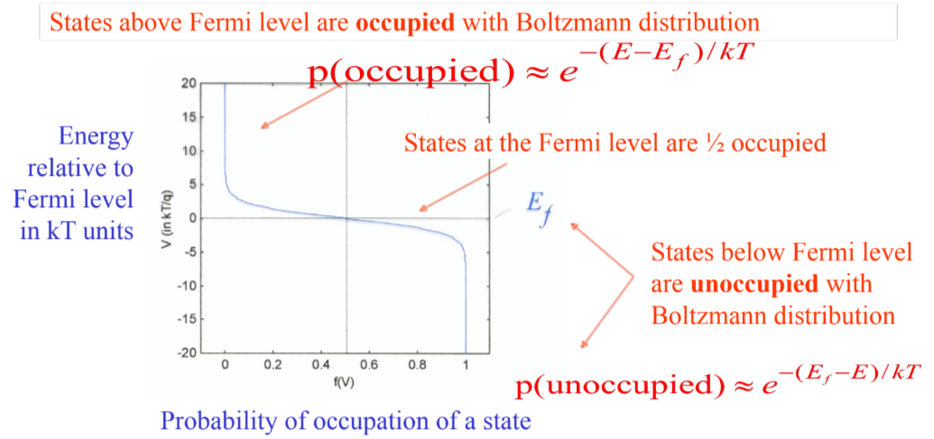
This probability distribution is the reason for the exponential characteristics of diodes and transistors.
In Thermal equilibrium (no external voltage applied and no net current flow), the total electron density in the conduction band is:
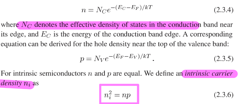
The law of mass action: $np=n_{i}^2$ :In equilibrium, more holes means less electrons.
For silicon:
- The effective density of states is $N_{C}=2.80 \times 10^{19}cm^{-3}$
- The intrinsic carrier density is $n_{i}=1.45 \times 10^{22}cm^{-3}$ at room temperature
- The concentration of $Si$ atoms in a crystal is $5 \times 10^{22}cm^{-3}$
- Which means only one out of $3\times10^{12}$ atoms is ionized at room temperature therefore conductivity is very low.
Energy band diagram, density of states, fermi dirac and carrier concentrations for intrinsic semiconductors at thermal equilibrium
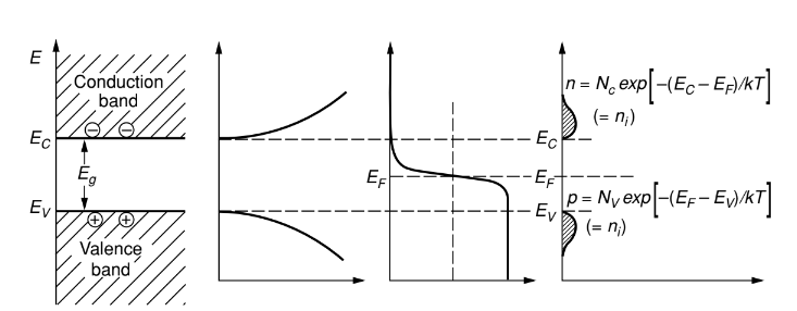
Note $n_{i}=n=p$
Impurity doping
We can significantly increase the conductivity of a semiconductor by impurity doping it.