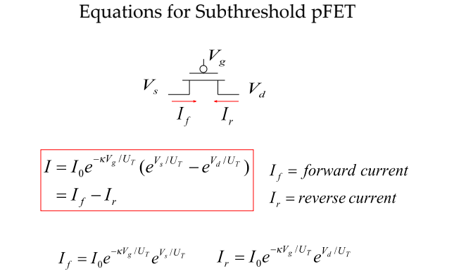
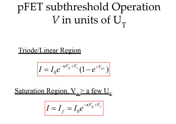
MOS transistors
Metal oxide semi-conductors use insulated gates to controlo barrier energies at PN surface junctions at source and drain.
Electron transport
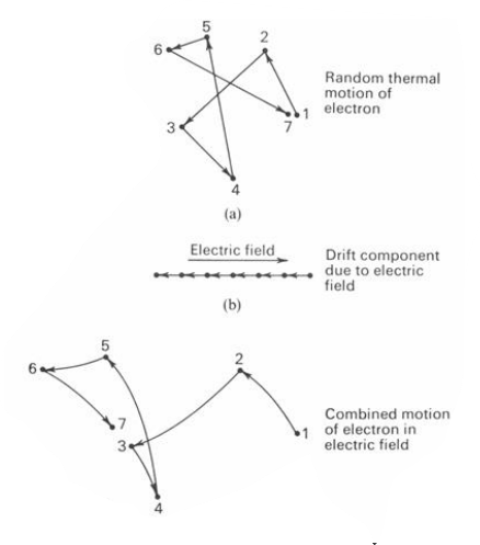
Drift
An electric field causes carriers to drift
$J_{drift} = qn\nu = qn\mu(\zeta)$
where:
- $J_{drift}$ is the current flux
- $qn$ is the charge density ($q$ is the elementary charge)
- $\nu$ is the velocity
- $\mu(\zeta)$ is the mobility function of the electric field
Illustration of the concept:
Diffusion
A density gradient causes carriers to diffuse. (When to doped types are put in contact for example)
$J_{diff} = -Dq\nabla n$
where:
- $D$ is the diffusion constant
- $\nabla n$ is the spatial gradient of charge density
Drift and diffusion are related by the Einstein Relation:
$D=\frac{kT}{q}\mu$
It expresses the connection between the diffusion constant $D$ which determines the forward and reverse currents, the mobility constant $\mu$ which determines the conductance of the resistor and the thermal voltage $\frac{kT}{q}$.
At $T=0$ , well... $D=0$ and there are no internal diffusion currents.
Thermal equilibrium
In thermal equilibrium (no external voltage applied), diffusion and drift currents are balanced ($J_{n}=J_{p}=0$)($J_{n}=J_{n,drift}+J_{ndrift}$ and so on for hole doped).
P-N Junction
What happens at a junction between P and N (physical contact)?
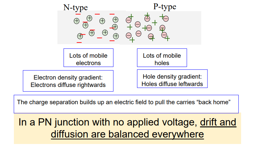
- The diffusion processes give rise to:
- A net electron flow from the n-type region to the p-type region.
- A net hole flow from p-type region to n-type region.
- This results in a diffusion current desity $J_{diff}=J_{n,diff}+J_{p,diff}$ from the p-type to the n-type
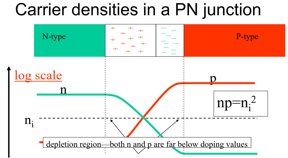
- The diffusing minority carriers recombine with majority carriers in the vicinity of the junction $\rightarrow$ this region is devoid of mobile charge carriers. ($np\ll n_{i}^2$) The Depletion region.
- On the n-type side of the junction, the donor electrons are absent and the donor atoms have a surplus proton. (+) charged side
- On the p-type side of the junction, the acceptor holes are filled by the donor atom's electrons and the acceptor atoms have a surplus electron. (-) charged side
- An electric field builds up in the depletion region that points from n to p.
- The electric field generates electron and hole drift currents from n to p.
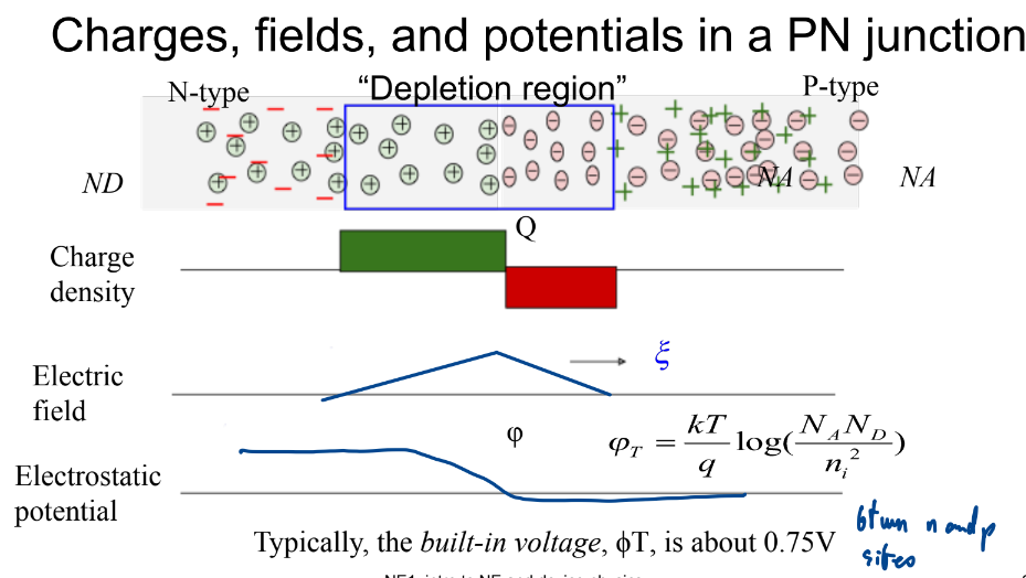
Electrostatic Potential: potential energy of positive charge (electron is the mirror image)
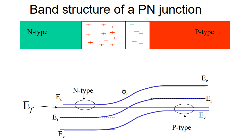
Band structure
I-V Characteristics
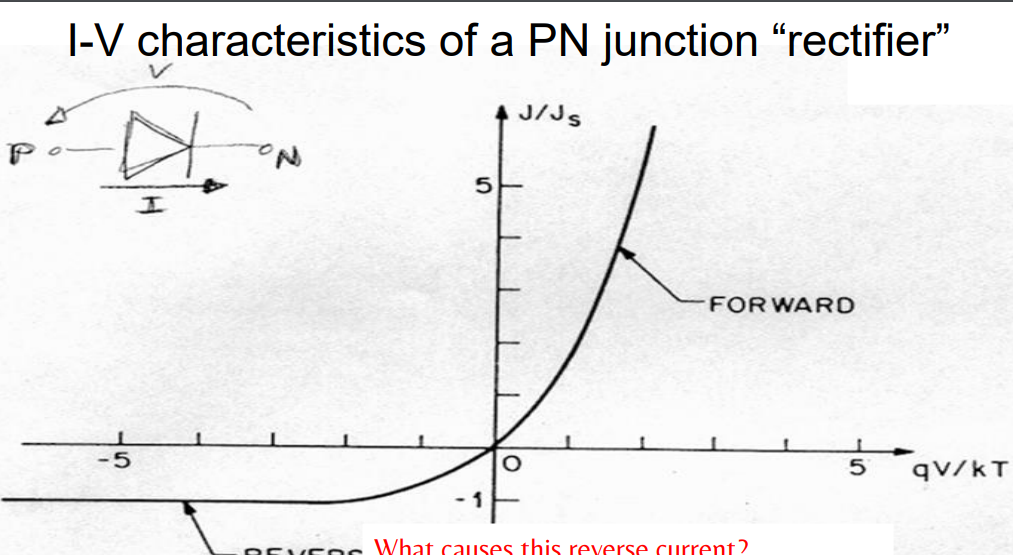
How do we generate a net current flow through the diode?
- We change the boundary conditions for the n and p type regions through external application of potential differences.
- If a positive voltage is applied to p, relatively to n the potential difference is called a forward biais
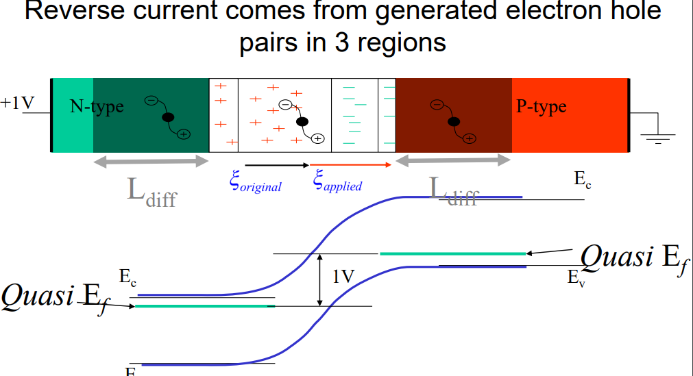
- If the voltage on n is higher than p, it is a reverse biais.
- Current flowing from p to n is a forward current
- Current flowing from n to p is a reverse current
- The electron current in the n region is transformed to a hole current in the p region.
- The applied voltage changes the built in voltage and modifies the width of the depletion region and the minority carriers outside the depletion region.
Structure
Biaising
Regimes
Body effect
pfet