Transconductance amplifier
Summary
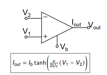
Input: $\Delta V =V_{1}-V_{2}$
Output: $I_{out}=g_{m}(V_{1}-V_{2})$
Settings: $V_{b}$ for $I_{b}$
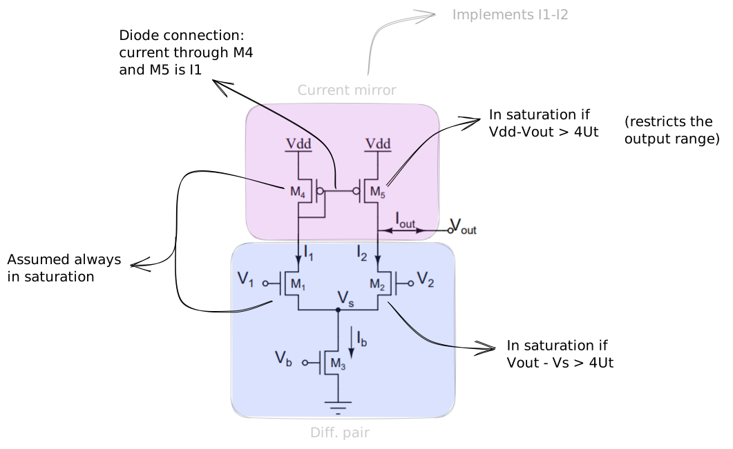
Notes: For it to work $M_{3}$ (and all transistors) must be in saturation. The diff pair must be in subthreshold.
Can be used as a differential voltage to current converter or a voltage amplifier.
%%🖋 Edit in Excalidraw, and the dark exported image%%
Current converter

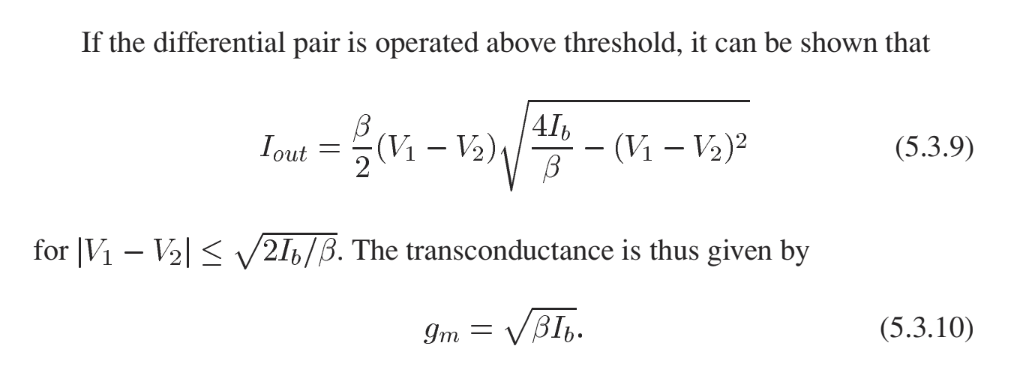
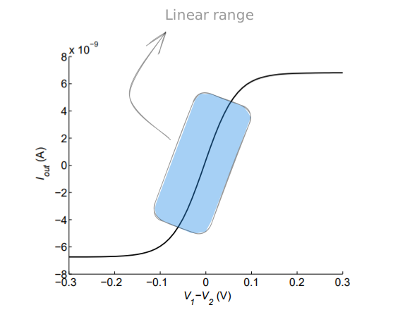
For small differential voltages (e.g. $|V1 − V2| < 200mV$), the tanh(·) relationship is approximately linear and can be reduced to a linear one:
$I_{\text {out }}=I_b \tanh \left(\frac{\kappa}{2 U_T}\left(V_1-V_2\right)\right)$
$I_{\text {out }} \approx g_m\left(V_1-V_2\right)$
$g_m=\frac{I_b K}{2 U_T}$
%%🖋 Edit in Excalidraw, and the dark exported image%%
$g_{m}$ is the transconductance of the amplifier (it has the dimensions of a conductance), but the output conductance is:
$g_{d}=-\frac{\delta I_{out}}{\delta V_{out}}=\frac{I_{b}}{V_{E}}$
where $V_{E}$ is the early voltage of $M_{2}$ and $M_{5}$.
Voltage amplifier
- Open circuit voltage gain (increases with the early voltage):
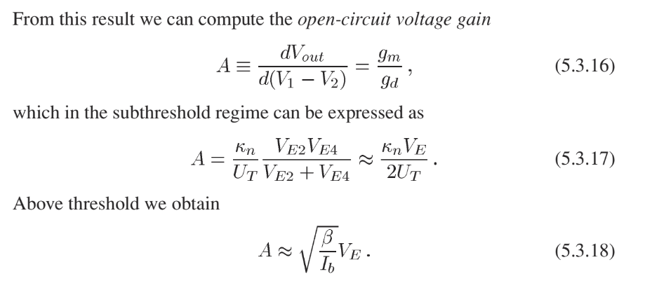
$Vout$ increases with $V_{1}$ and decreases with $V_{2}$ the gate of $M_{1}$ is called non-inverting (+) input terminal and the gate of $M_{2}$ is called inverting input terminal (-).
Often the amp is used as a comparator: outputs a high voltage if $V_{1}>V_{2}$ and a low voltage if $V_{1}<V_{2}$.
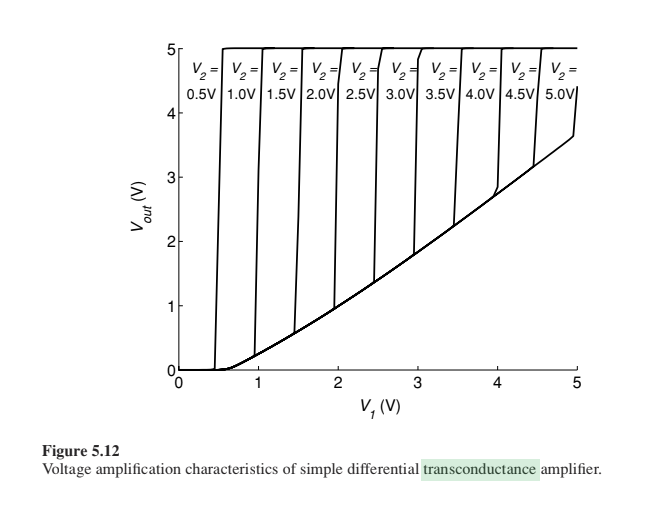
Output voltage limits
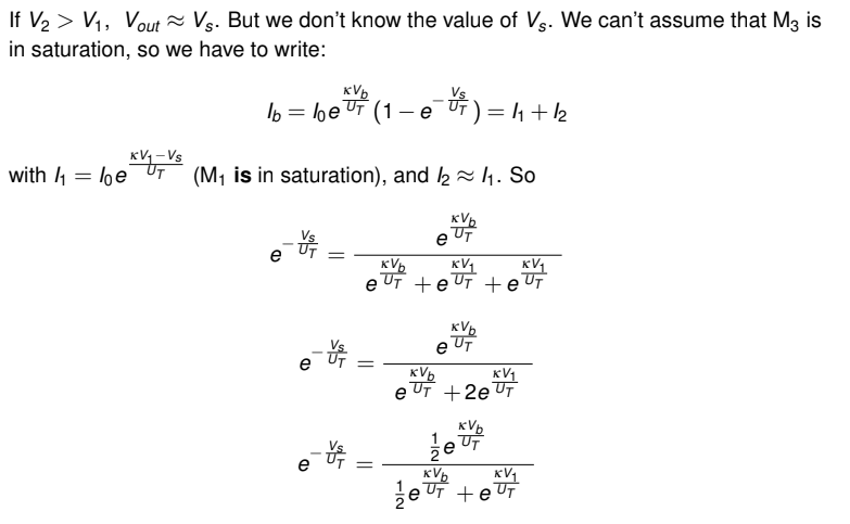
Since in the open circuit is normally at one of its limits, we will now determine where those limits lie. If $V_{1}$ is larger than $V_{2}$ , $M_{4}$ goes out of saturation. And we get this shite:
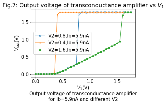
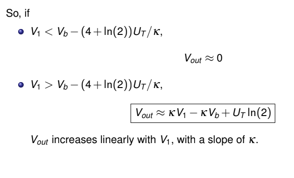
Varying V2 highly influences when Vout will make the switch (of course), we can also see that the bigger V2, the longer Vout increases linearly with V1 (with a slope of kappa).
The output range is restricted to:

In order tom keep M5 and M2 in saturation.
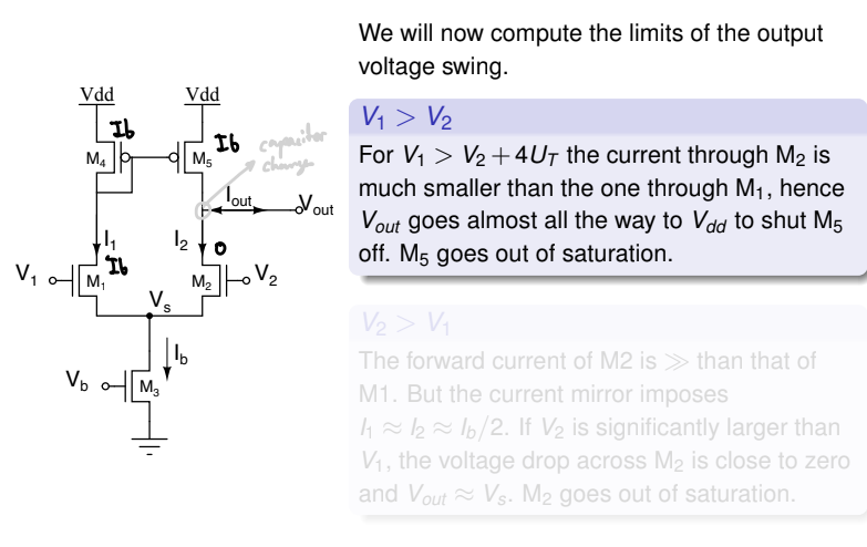
For V1>V2:
I1 is equal to Ib and I2 is 0, therefore the current in the mirror is Ib which will lead to charging of the "node capacitor" and eventually M5 will go out of saturation as Vout will go up to Vdd.
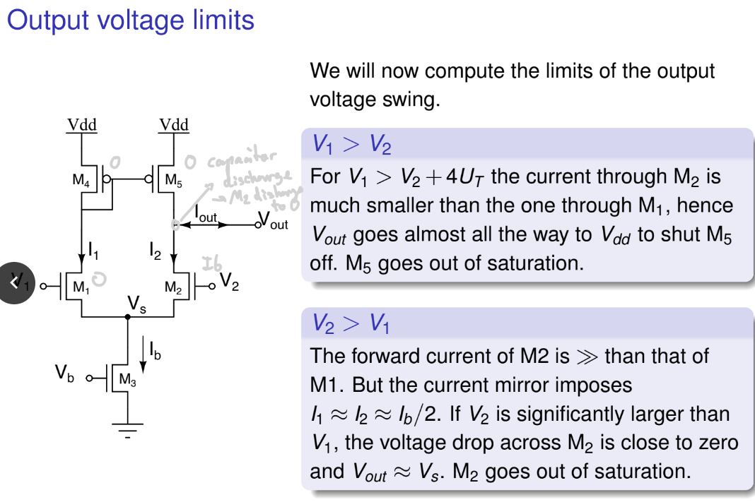
For V1<V2:
V2 is equal to Ib and I1 is 0, therefore the current in the current mirror is also 0. Which will lead to a discharge in the "node capacitor" and the M2 NFET voltage will drop to 0 and as M2 goes out of saturation,Vout≈Vs.
Wide range transamp
The current $I_{2}$ is mirrored twice such that the output stage is symmetric and decoupled from the input stage. This decoupling also allows the design of output stages with large open-loop gains or large output currents. Disadvantages of this extension are the need for almost twice as many transistors as for the basic version, and the increased effect of mismatches due to fabrication tolerances.
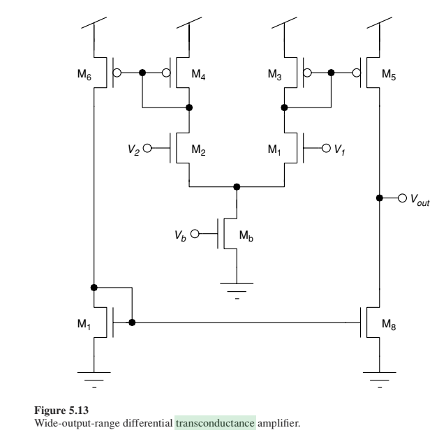
The current mirror transistors, in order be in saturation need a $Vds$ that is lower than $Vdd−4UT$so Vs must satisfy this condition as well. $Vs$ must also keep M3 in saturation and must therefore be greater than $4UT$. We end up with $I1$ charging the "capacitor node" at $Iout$ and $I2$ discharging it. And the only boundary on Vout is then $4UT$